
HDI PCB fabrication,
from 4 layers to 32,
at 45,000 m² a month.
Six lines, one MES record per panel. Laser-drilled microvias, via fill, sequential lamination and impedance control live on the same floor as our AOI, flying-probe and X-ray test cells.
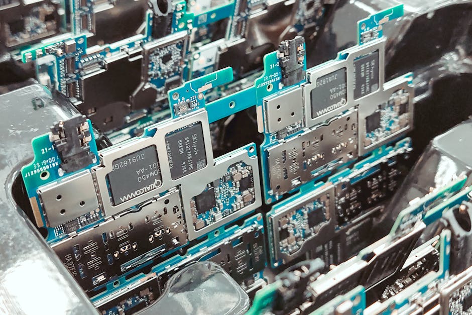
Nine controlled stages, one serial number.
DFM & engineering review
Every Gerber is checked against our design rules within 26 hours — annular ring, aspect ratio, drill-to-copper and panel utilisation.
Inner-layer imaging & etch
LDI exposure and automated optical inspection of every inner layer before lamination — no optical escapes forward.
Sequential lamination
Vacuum presses with per-cycle profiling, up to four build-up cycles for any-layer HDI stack-ups.
Laser drilling & via fill
UV laser microvias down to 50 µm, copper-filled and planarised for stacked and via-in-pad structures.
Plating & backdrill
Copper plating to controlled thickness, with depth-controlled backdrilling for high-speed signal integrity.
Outer layer & solder mask
LDI outer imaging, 40/40 µm L/S capability and LPI solder mask in matte black, green, blue or white.
Surface finish
ENIG, ENEPIG, immersion silver and tin, hard gold and OSP — all with thickness verification per lot.
Electrical test
Flying probe to 40,000 nets, impedance coupons, TDR verification and 100% continuity on Class 3 builds.
Final QA & packing
Microsection, ionic cleanliness, AOI sign-off, moisture-barrier packing and lot-level traceability records.
The tolerances we quote.
| Parameter | Standard build | Advanced build |
|---|---|---|
| Layer count | 4 – 16 layers | 18 – 32 layers |
| Line width / spacing | 100 / 100 µm | 40 / 40 µm |
| Microvia diameter | 100 µm laser | 50 µm laser, filled |
| Copper thickness | 1 – 2 oz | 3 – 12 oz heavy copper |
| Board thickness | 0.6 – 2.4 mm | 0.4 – 6.0 mm |
| Maximum panel | 18" × 24" | 21" × 25" |
| Impedance control | ±10% | ±8% with TDR report |
| Lead time | 5 – 15 working days | 72-hour prototype |
Every panel
watched by
a model.
Our AOI and ACI cells feed a defect-classification model trained on three years of our own production images. Escape rate is 0.8% and falling — and every catch is tied back to a process parameter.
Laminates, finishes and stack-ups we run daily.
FR-4 High Tg (170–180°C)
The workhorse for multilayer digital and industrial boards. Halogen-free options available with UL 94 V-0 rating.
- — Tg 170°C / Td 340°C
- — Dk 4.2 – 4.6 @ 1 GHz
- — CTE 45 – 55 ppm/°C
- — 4 – 32 layers, 0.4 – 6.0 mm
- — Isola, Shengyi, Kingboard qualified
- — Bonding, prepreg and thin-core stock
- — Copper to 12 oz on request
- — IPC-4101 slash sheets on file
Polyimide & rigid-flex
For boards that fold, flex or live above 150°C. Adhesive-less constructions to IPC-6013 Type 3 and 4.
- — 1 – 8 flex layers
- — Coverlay, LPI or photo-imageable
- — Dynamic bend to 100k cycles
- — Rigid-flex hybrids with 6:1 stiffness transition
- — EMI shielding films
- — Stiffeners in FR-4, FR-4 and stainless
- — Controlled impedance on flex
- — 3D-bent form tooling support
RF, PTFE & microwave
Low-loss antenna, radar and radio boards using PTFE, hydrocarbon and mixed-dielectric builds.
- — Dk 2.2 – 10.2, Df to 0.0009
- — Rogers, Taconic, Isola qualified
- — Mixed dielectric with FR-4 cores
- — Operation verified to 40 GHz
- — Cavity and air-gap constructions
- — Press-fit and edge-launch transitions
- — Plated through-hole on PTFE
- — S-parameter coupons on request
Metal core & IMS
Thermal management for LED, power conversion and motor-drive electronics with aluminium or copper bases.
- — Aluminium 1.0 – 3.2 mm base
- — Copper base for 400°C excursions
- — Thermal conductivity 1 – 8 W/m·K dielectric
- — Thermal vias and direct-bonded copper
- — Single and double-sided IMS
- — Multilayer metal-core hybrids
- — CNC routing and countersink
- — Thermal imaging verification per design
What we can commit to, in writing.
Quick-turn prototypes
Up to 8 layers, 1–20 pieces, free DFM review, DHL express included on standard destinations.
HDI series ramp
Any-layer HDI from release to first article, with PPAP packs for automotive programmes.
Monthly unit ceiling
Serial production with reserved capacity, VMI and bonded stock agreements.
Upload a
stack-up.
Send your Gerbers and drawing notes. We will return a DFM report, a firm price and a dated lead time.